Miniaturization Trends Driving PCB Mounted Terminal Innovation
As electronics evolve toward smaller, faster, and more multifunctional devices, the demand for miniaturized PCB mounted terminals is rapidly increasing. These components are no longer passive links but precision-engineered elements that directly influence reliability, efficiency, and manufacturability.
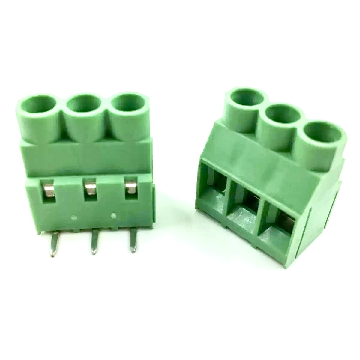
Compact Design Challenges in Modern PCB Assemblies
Shrinking device size means every millimeter of PCB real estate counts. PCB mounted terminals must now support:
-
High pin density without compromising insulation resistance.
-
Thermal stability to withstand heat from dense component layouts.
-
Ease of assembly in automated SMT and reflow soldering environments.
Manufacturers are innovating with low-profile housings, optimized plating materials, and reinforced geometries to ensure performance under these constraints.
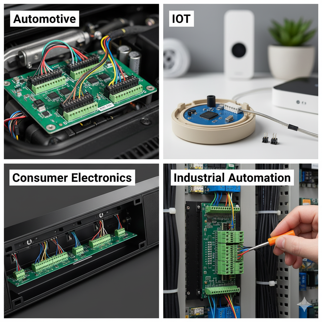
Application-Specific Requirements Across Industries
Miniaturized PCB terminals are not universal; each industry imposes unique design requirements:
-
Automotive electronics: High vibration resistance and temperature tolerance for ECUs and ADAS modules.
-
IoT and wearables: Ultra-compact profiles for battery-powered devices with limited space.
-
Consumer electronics: Quick assembly designs that enable high-volume manufacturing.
-
Industrial automation: Higher current capacity despite compact size, ensuring safe operation in demanding conditions.
This diversity drives the need for OEM flexibility in terminal block design, often requiring custom materials and configurations.
Materials and Engineering Choices Shaping Performance
The choice of plating materials—such as tin, nickel, or gold—directly impacts long-term stability. Tin plating is cost-efficient, nickel offers corrosion resistance, while gold enhances conductivity for mission-critical circuits. Housing materials like high-temperature polymers further protect against reflow processes.
To highlight differences:
| Feature | Miniaturized PCB Terminals | Conventional PCB Terminals |
|---|---|---|
| Profile Height | <5 mm in compact designs | Typically >7 mm |
| Pin Density | High-density, fine pitch | Standard pitch spacing |
| Application Focus | IoT, automotive, wearables | General-purpose electronics |
| Assembly Compatibility | Optimized for SMT, reflow | Often through-hole only |
This comparison underscores how miniaturization is less about replacing older terminals, and more about meeting new performance demands.
Practical Q&A from Buyers and Engineers
Q1: Can miniaturized PCB terminals still handle high currents?
Yes. While smaller, reinforced copper alloys and advanced plating allow certain models to carry comparable currents to larger designs.
Q2: How does miniaturization affect repair and replacement?
Designers often specify modular or plug-in styles, making rework possible even in tight layouts.
Q3: Are miniaturized terminals more expensive?
Unit costs may be slightly higher due to precision tooling, but savings in board space and device size often offset this.
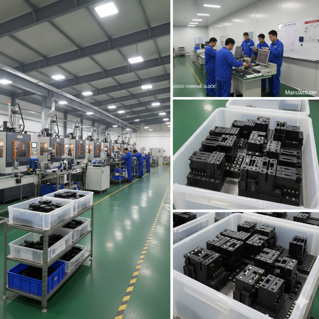
Why ZhongBo Leads in Miniaturized PCB Terminals
At ZhongBo, we engineer PCB mounted terminals tailored for miniaturization trends, offering:
-
Customized designs for IoT, automotive, and compact consumer electronics.
-
Certified plating and housing materials to balance reliability with cost efficiency.
-
Scalable production capacity to support both prototyping and global supply chains.
As electronics continue to shrink, our focus is on delivering components that maximize performance in the smallest possible footprint. Learn more about our solutions at ZhongBo’s homepage or connect with us directly via our contact page